In more detailed article the same authors suggest 0.762mm thick substrate with relative dielectric constant e_r = 2.6 and tan_delta=0.0025. The dimensions of antenna are: W1=2.06mm, W2=16.25mm, L=36.58mm. Shorting pins located at either end of antenna have a 0.5mm radius. Antenna is fed with a probe at the junction of the first narrow line and the next wide section meet. The dielectric material extends out 2.0 mm from each side and 2mm from each end.
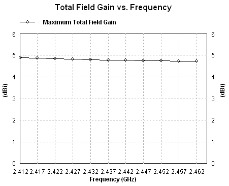
Authors reports that FDTD simulated antenna gain showed 6.4dBi. Measured with the above geometry was 4.6dBi (1.8dB less than simulated). In the first article better results were reported. Calculating stripline properties shows, that second article uses non optimal stripline dimensions?
The following program may be useful for simulation and PDF generation for PCB etching. Width W1 is calculated for equivalence of 50 ohm transmission line. Width W2 should be slightly greater than 5 times of W1. Length of the microstrip line is equivalent to 1/2 wavelength.
Default dimensions are for 1.5mm thick FR-4 substrate with dielectric constant (relative permittivity) eps_r = 4.2. Center frequency is assumed to be 2437 MHz. For other substrate properties use microstrip calculator.
cat > film.pdf and then
paste the file contents into terminal with Ctrl-D at end. For
larger antenna configuration you should adjust /MediaBox[]
and the number of segments. Similar procedure for pasting
into cmd window is copy con oma.3dt and
Ctrl-Z for stream close after paste.
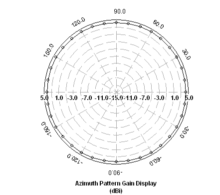
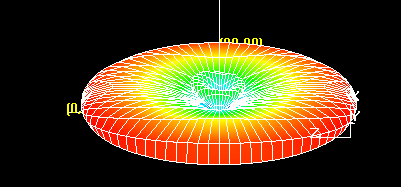
For this microstrip antenna IE3D from Zeland seems to be the obvious choice. But only the latest version supports finite substrate and finite ground. Fidelity is more general for antenna simulation but more time consuming as it works on finite differences method in time domain. You can easily end up with million of grid cells and 150000 time steps with high gain antenna. This means hours of simulation. The first figure near the input form shows 3D configuration in Fidelity. Nearby is sample current display from IE3D. Here is sample object list for Fidelity:


Upper figure shows flat geometry and coordinate system recommended for simulation of this kind of antenna. Approx 2800 cells and more than 400MB memory was required for IE3D process.
After conversation with Zeland support I've come to conclusion that finite dielectrics will not perform well with OMA simulation:
The infinite substrate model may neglect some effects of the finite substrates. However, its solution has a better matching to reality for the majority of the substrate interface. Using finite substrate, it may cause inaccurate resonant frequency if the meshing is not aligned. Also, this structure is quite big, using finite substrate may create too many unknowns for it. I strongly suggest you to use IE3D's infinite substrate model for it.
FR4 is commonly available laminate. It is suitable for this kind of design. The only difficulty with this substrate is that dielectric constant varies among producers/frequency. The best common guess is 4.2, but the range is 4.2-4.8 and varies with the glass/epoxy ratio of the materials used. I suggest to design strip line for center frequency 2.437 GHz and then find the best frequency on site. See also this tech-tip for comments on FR-4 dielectric constant.


This interesting design with 5.0 to 6.1dBi is taken from IEEE Transactions on Antennas and Propagation,vol.52,no.2,February 2004 pp 624--62 by K.Wong et.al. PCB dimensions of this small antenna are 176x16mm. More detailed schematic from article is here. Feedpoint can be easily attached to H-155 coax. Center frequency can be moved with S parameter and can vary from S=85mm for 2.552 GHz to S=220mm for 2.352GHz. The best results were measured for S=96mm, W=6mm, L=25mm at f_r=2.436 GHz. Simulation with HFSS showed 7.4 dBi (5.5 dBi measured). VSWR is better than 1:1.5
Dielectric constant (permittivity) 4.4 on 0.4mm FR4 laminate is assumed, but thic can vary substantiali from manufactures pair-to-pair measuring on different WLAN channels is suggested to obtain maximum gain.
I've done some PCB layouts with 1 mil resolution. Sample Color PDF and Color EPS and ZIP archive with EPS files are available for etching in half dozens.
Note for "home alone" testers: This is "no joke" PCB on 0.4 FR4 laminate. Some lines are with 8mil thickness! Take care of the film mirroring. No drilling tough.
Some symetric tests done by me with two Asus WL-500 GX at distance 700m with two OMA dipole antennas attached with 1.5m H-155 cable. Radio Power 65mW, 1-2 Mbps, Data rate 6 Mbps. Seven tests with chanell hopping to compensate ambient fluctuations were performed in april 2004.
chan   RSSI1   RSSS2   RSSI3   RSSI4   RSSI5   RSSI6   RSSI7
1       -81     -78     -85     -85     -85
2       -79                     -83
3       -78     -81                     -80
4       -78             -80     -79             -79     -79
5       -76     -79                     -78     -78     -78
6       -76                     -76             -76     -76
7       -76     -76     -76             -76     -76     -76
8       -77                     -76             -76     -76
9       -77     -78                     -76     -77     -76
10      -78             -79     -79             -79     -79
11      -79     -79                     -79
12      -78                     -78
13      -79     -79     -78             -78
From results you can see that the best channels are 6 and 7 and that OMA dipole is well tuned in the middle of the band. Some preliminary comparison tests done by dplant are available here .